Chinese Researchers Make Progress in Atomic Layer Bonding Contacts for Two-Dimensional Semiconductors
Supported by the National Natural Science Foundation of China (Grant Nos: 52225206, 92163205, 52188101), the team led by Academician Yue Zhang and Professor Zheng Zhang from the University of Science and Technology Beijing (USTB) has made a breakthrough in the field of two-dimensional (2D) semiconductors and their application in integrated Circuits (ICs). Their achievement, entitled “Atomic layer bonding contact in two-dimensional semiconductors”, was published online in the journal Science on November 21, 2025. Link to full text: https://www.science.org/doi/10.1126/science.adz2405.
In the field of ICs, achieving excellent metal semiconductor contact is a great challenge in device manufacturing. In traditional semiconductor device manufacturing, researchers construct transistors with low contact resistance, high thermomechanical stability, and excellent thermal/electric conductivity by creating strongly bonded metal-semiconductor contact interfaces to meet application requirements. However, for 2D transition metal chalcogenide (TMD) materials that lack dangling bonds on their surfaces, achieving strong bonding contact with metal electrodes poses a significant challenge in the development of advanced process ICs.
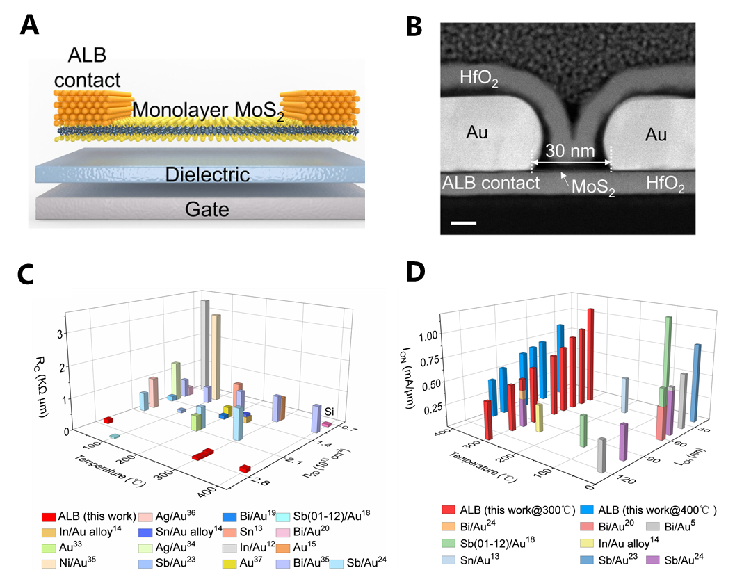
To promote the engineering application of 2D semiconductors in ICs, Prof. Yue Zhang and colleagues proposed a new paradigm of atomic layer bonding (ALB) to address the core challenges of metal 2D semiconductor contact. By accurately removing sulfur atoms from the surface of molybdenum disulfide (MoS2) and directly depositing metal electrodes, a stable contact interface between transition metal monolayers and metal electrode atomic layers has been successfully constructed. This strategy synchronously achieves precise control of electronic structure and lattice structure, ultimately forming an atomic layer bonding contact interface that combines strong band coupling and high bonding strength. As a result, MoS2 transistors have achieved contact resistance as low as 70 Ω μm approaching the theoretical limit and thermomechanical stability as high as 400℃, meeting the requirements of high-performance electronic devices in the International Roadmap for Devices and Systems (IRDS).
For the first time, this study has achieved atomic layer bonding between 2D semiconductors and metal electrodes, yielding contact resistance approaching theoretical limits and superior electrical transport properties that are maintained through high-temperature processes. This is a key progress in expanding 2D semiconductor devices from laboratories to wafer fabs.

Figure Comparison of structure and performance of atomic layer bonding (ALB) contact transistors. (A) Schematic diagram of transistor structure. (B) Cross sectional morphology of MoS2 transistor with short channel. (C) Comparison of contact resistance of MoS2 transistors (red for this work). (D) Comparison of on state current of MoS2 transistors (red and blue represent the performance of this work after heat treatment at 300℃ and 400℃, respectively).
Contact Us

National Natural Science Foundation of China
Add: 83 Shuangqing Rd., Haidian District, Beijing, China
Postcode: 100085
Tel: 86-10-62327001
Fax: 86-10-62327004
E-mail: bic@nsfc.gov.cn
