Chinese Scholars Made Progress in Wafer-Scale Fabrication of Two-Dimensional Semiconductor Wafers
With support from the National Natural Science Foundation of China (Grant Nos. 52025023, 52322205, 52250398), Professor Kaihui Liu from Peking University and his collaborators have made a major advance in fabrication of high-quality two-dimensional (2D) indium selenide (InSe) semiconductor wafers. The research, titled “Two-dimensional indium selenide wafers for integrated electronics,” was published online in Science on July 18, 2025. (Full article link at https://www.science.org/doi/10.1126/science.adu3803).
With the exponential growth in demand for computing power in cutting-edge applications such as artificial intelligence (AI) and the Internet of Things (IoT), traditional silicon-based transistor technologies are approaching their physical limits at sub-10-nanometer nodes. This limits improvements in performance, energy efficiency, and integration density. Thus, the development of novel semiconductor channel materials has become imperative to break through the bottlenecks of silicon-based technologies and sustain the advancement of next-generation integrated circuits.
Among emerging candidates, InSe stands out as a promising material tosurpass the performance ceiling of silicon, due to its ultra-low electron effective mass, high thermal velocity, and suitable bandgap. InSe exhibits theoretical performance that not only surpasses silicon but also exceeds other 2D semiconductors, with its potential demonstrated in proof-of-concept devices. However, its integration at the wafer scale has long remained a challenge, posing a critical bottleneck to its industrial application.
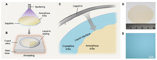
The research team proposed a novel solid–liquid–solid growth method and successfully overcoming the key challenge of achieving high-quality InSe wafers. An indium-rich liquid interface was created using a liquid indium seal around the wafer to drive the conversion of amorphous InSe into crystalline InSe, resulting in the production of 2-inch wafers with uniform thickness, pure phase, and high crystallinity. Transistor arrays fabricated on the InSe wafers demonstrated outstanding electronic performance, including an extremely high mobility (averaging as high as 287 cm2 V-1 s-1) and a near-Boltzmann-limit subthreshold swing (averaging as low as 67 mV/dec). Key parameters of InSe devices with ultrashort gate lengths (below 10 nm) exceeded those of the state-of-the-art Intel 3-nanometer node technology.
This work has achieved the wafer-scale fabrication of high-quality 2D semiconductors, advancing the development of next-generation computing and communication technologies with high performance and low power consumption. It holds great promise for enabling key applications in cutting-edge fields such as artificial intelligence, autonomous driving, and smart devices.

Figure. Solid–liquid–solid growth strategy for the growth of high-quality wafer-scale InSe single crystals
Contact Us

National Natural Science Foundation of China
Add: 83 Shuangqing Rd., Haidian District, Beijing, China
Postcode: 100085
Tel: 86-10-62327001
Fax: 86-10-62327004
E-mail: bic@nsfc.gov.cn
