Chinese scholars made progress in atomic manufacturing of rhombohedral two-dimensional single crystals
Under the support of the National Natural Science Foundation of China (Grant Nos. 52025023, 52322205, 52250398), Professor Kaihui Liu’s research group from Peking University, in collaboration with Associate Professor Can Liu’s research group from Renming University of China and Professor Guangyu Zhang’s research group from Chinese Academy of Sciences, have realized the atomic manufacturing of rhombohedral two-dimensional (2D) single crystals. The research achievement titled “Interfacial epitaxy of multilayer rhombohedral transition metal dichalcogenide single crystals” was published in Science on July 5, 2024. (Full article link at https://www.science.org/doi/10.1126/science.ado6038).
2D transition-metal dichalcogenides (TMDs) are promising materials for ultrascaled transistors in next-generation electronic integrated circuits (ICs) and ultracompact components in photonic ICs. Theoretical analysis and experimental validation have consistently indicated that rhombohedral (3R) TMDs, compared to their monolayer and hexagonal (2H) counterparts, exhibit enhanced current density and higher carrier mobility, making them quite suitable for sub-5-nm node transistor channels. At the same time, the interlayer stacking manner of 3R-TMDs, which exhibits both broken in-plane inversion and out-of-plane mirror symmetries, enables switchable interfacial ferroelectricity, energy-efficient bulk photovoltaic effect, and constructive interference of nonlinear optical response. However, the production of 3R-TMD single crystal films for electronic/photonic chips is extremely challenging.
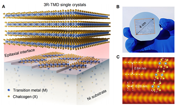
In response to these challenges, the aforementioned research teams proposed a new growth paradigm of “lattice transport-interfacial epitaxy”. By continuously delivered metals and chalcogens to the interface between a single-crystal nickel substrate and 2D materials to grow a consistent 3R-TMDs. In this process, the steps on the substrate surface are used to ensure single crystallinity and consistent stacking sequence, and for the first time, the universal preparation of wafer-scale 3R-TMD single crystals is achieved. Experimental results show that these materials exhibit extremely high electrical properties, meeting the semiconductor device mobility target of the International Devices and Systems Roadmap for 2028; at the same time, in terms of nonlinear frequency conversion, high-efficiency difference frequency conversion efficiency is achieved in the near-infrared range, which is 5 orders of magnitude greater than that of monolayers. This work has developed a new paradigm of “lattice transport-interfacial epitaxy” for material production, which is expected to promote the applications of the next-generation electronic and photonic chips.

Figure. “lattice transport-interfacial epitaxy” for the production of wafer-scale 3R-TMD single crystals
Contact Us

National Natural Science Foundation of China
Add: 83 Shuangqing Rd., Haidian District, Beijing, China
Postcode: 100085
Tel: 86-10-62327001
Fax: 86-10-62327004
E-mail: bic@nsfc.gov.cn
